
Designing in KiCad
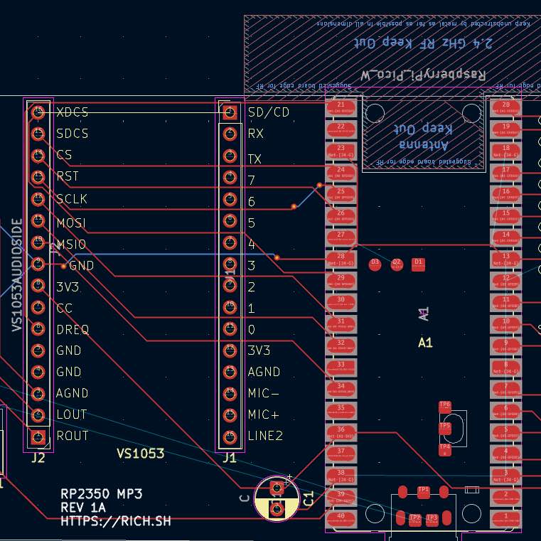
I worked to transfer the breadboard design from previous iterations into kicad. After several phases of rework - (and with further cleanup needed), I decided to just expose some extra GPIO and deal with the input board later. This way I could either use my I2C input or use some other input buttons.
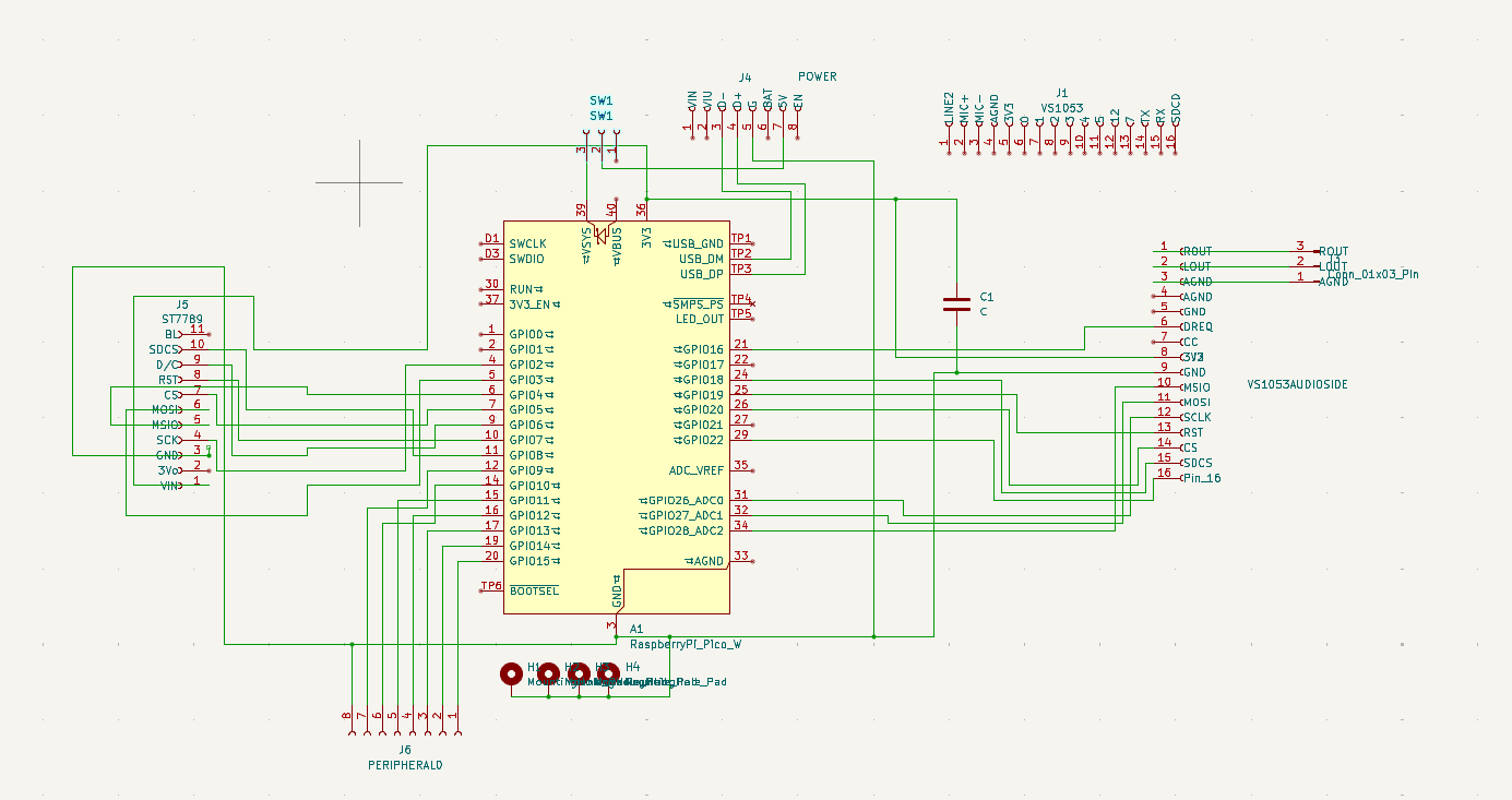
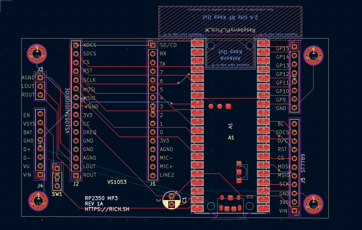
Then, I laid out the board. The main goal for this is - make something I can use sockets to be able to test & validate the major components, and give enough space for bodge wires and hacks in case I missed something in the first iteration.
For now, I’m planning to leave the test pads alone - but in the final version, I plan to add a board cutout with castellated pads to enable connection of the USB data pins (so firmware can be updated without opening the case).
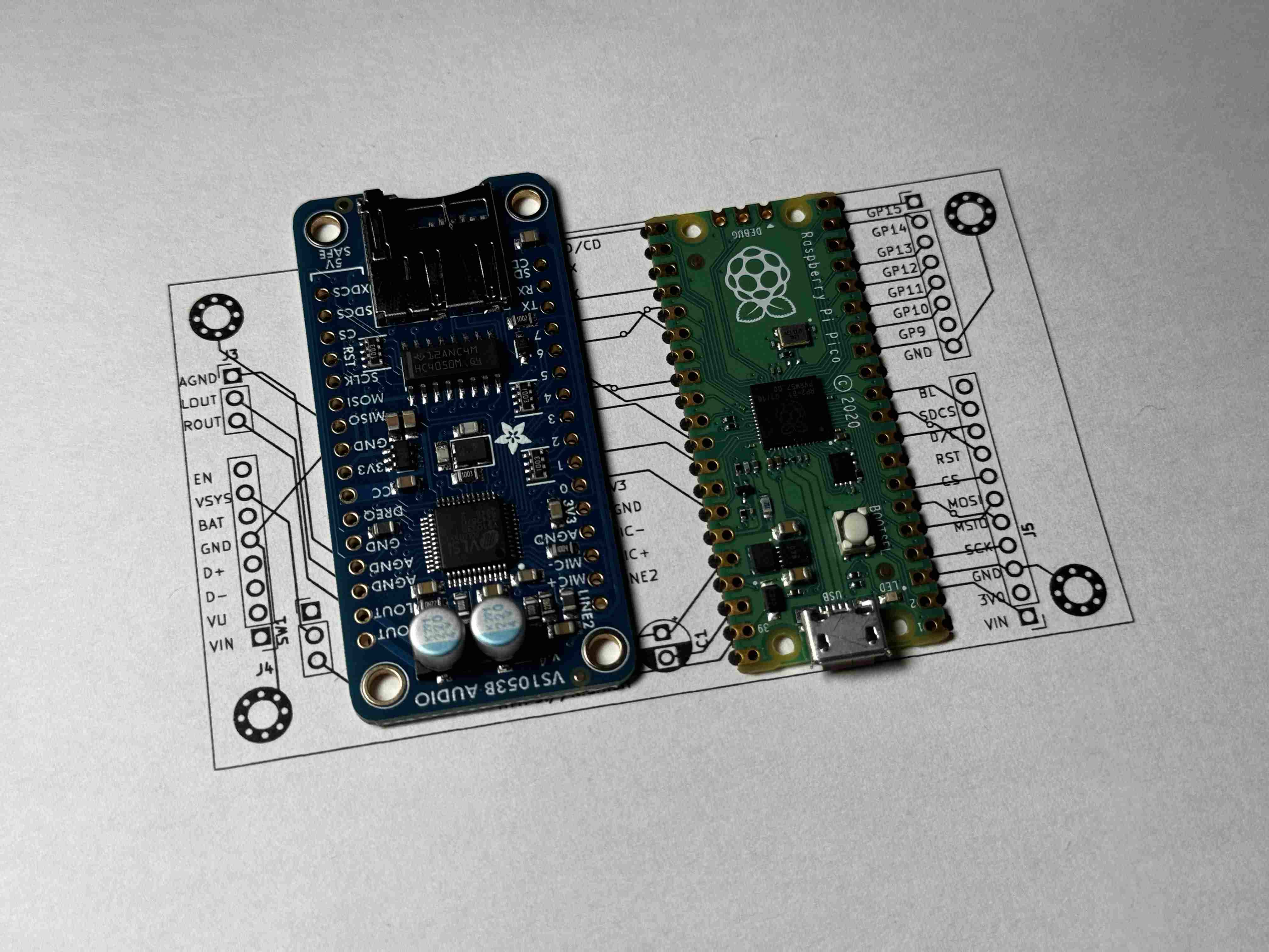
I then used my favorite technique for previewing the board - printing it 1:1 on my laser printer, and physically laying out the major components to ensure it all fits as expected
I will breadboard out the connections for the screen, buttons - so I can decide what my approach for those will be. The screen has a ribbon cable (Adafruit’s EyeSPI), so I’m debating if the final one will use pin headers, or use the ribbon cable to allow us to relocate the board elsewhere. There is potential that I do the ribbon cable approach for the final version, so that I can place the logic board on the bottom half, and put SMT buttons on the backside with the RP2350, VS1053, and charging circuits, etc - on the other.
The boards are on order, and I will update/report back once I have them assembled and working (hopefully, without too many bodge wires & hacks!)
Assembled Test Board
I assembled the board, then probed various points to compare versus the original. There was only one trace I need to reroute - the DREQ pin from the VS1053 was routed to the wrong GPIO pin on the pi. Not a big deal, and we could have just reconfigured the pin in software - but I’d rather keep it identical to the prototype for now.
For some reason, I had the bright idea to re-design the board’s input and outputs, funnily enough one of the pins originally wired to DREQ was used. I needed to slightly tweak my firmware so that I could use the I2C bus from the new pins. I also neglected to add an additional +3.3V pin near my I/O panel, which I will need to add in the production version. I’m thinking I’m going to keep the inputs modular. I could in theory use a matrix keypads (7 pins), which I purchased for another project to instead add a LOT of buttons and text input. Alternatively, I could wire up my own matrix with up/down/left/right/select/back buttons.
After using some stacking headers to alleviate clearance issues with the screen and battery circuits, it powered on successfully!:
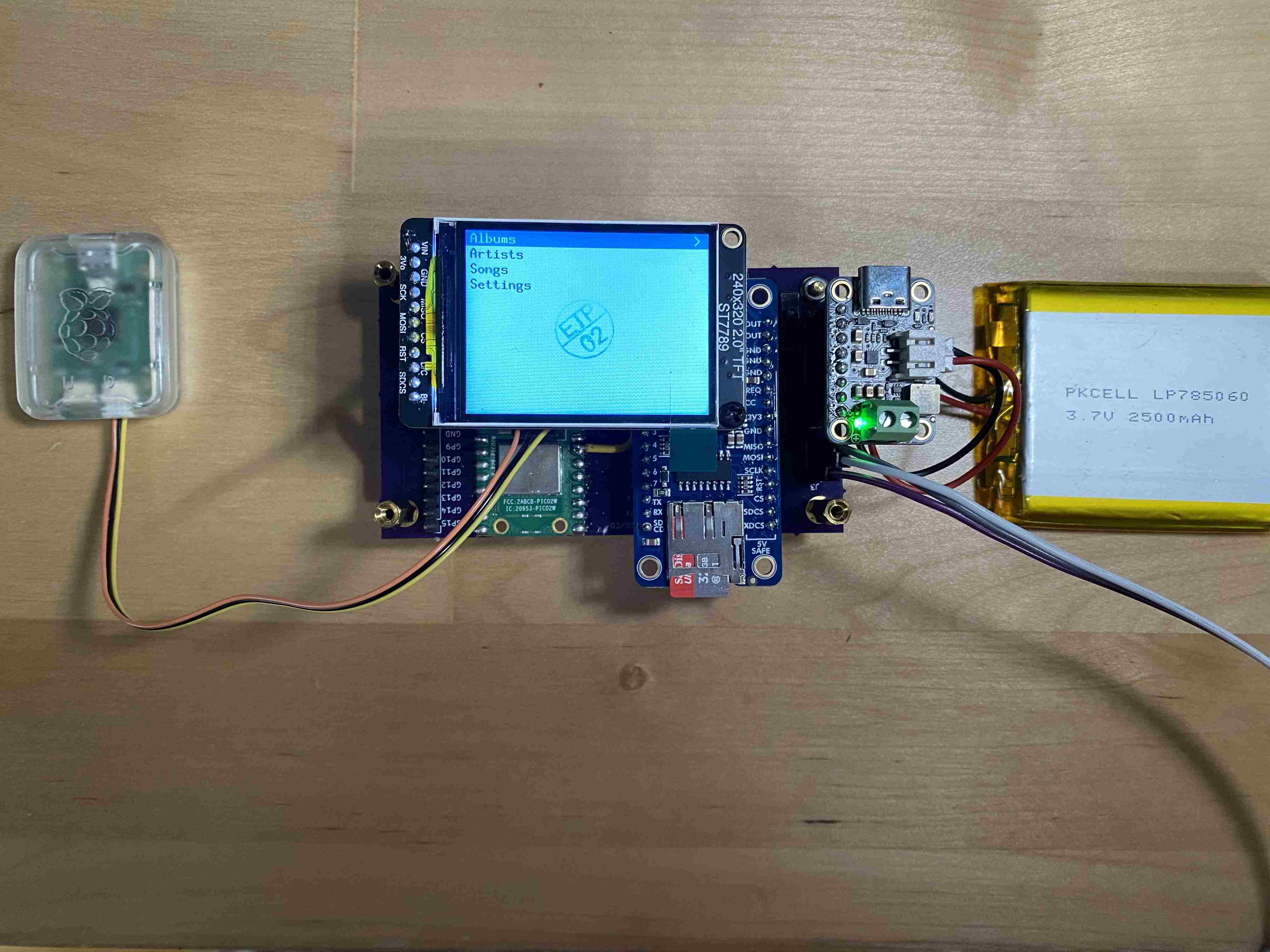
Upon testing - I encountered a new problem - the outputs seemed weak and distorted. Possibly related to traces crossing places they shouldn’t? no ground plane? Bad soldering on my DREQ bodge wire? No. As it turns out, I used a TRRS plug, and left the extra pin floating. Swapping for original TRS solved this. I spent quite a bit of time checking things (at first, I thought the rest of the DREQ trace was picking up interference from the data lines nearby).
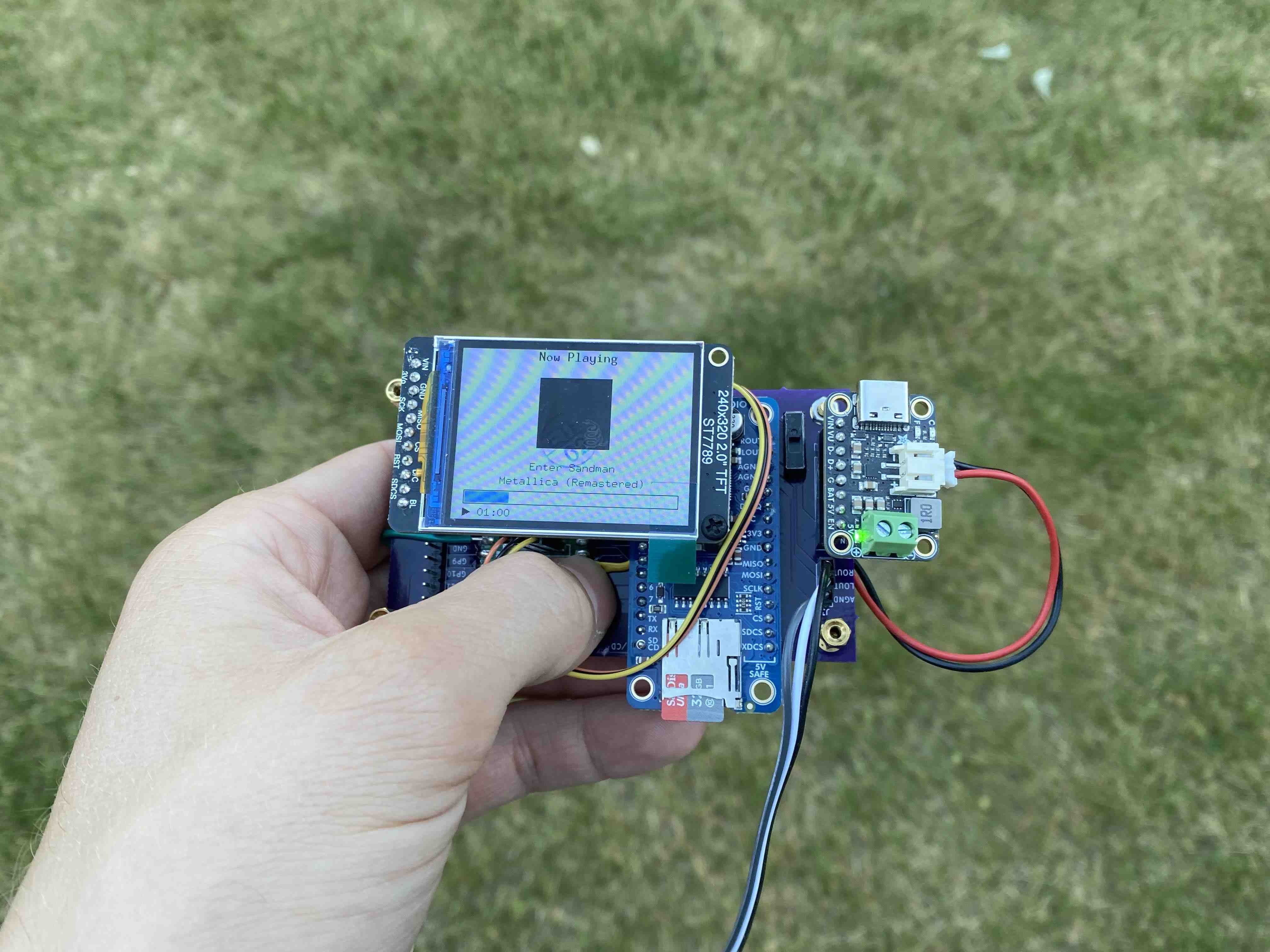
I think we’re ready to redesign this into something real. The current design is obviously not compact and is also not user friendly. I can’t exactly put this in my pocket:
User I/O
This was the part I left undefined. For now, I’ve decided to do both. I’m going to design a simple test button I/O board, to connect to my open GPIOs. I’m also going to expose a JST plug for my existing click wheel. With that I can prototype both, and leaves the most flexibility. The I2C bus needed only needs two pins (which are free). But buttons are definitely the simple way to go.
I spent a bit of time trying to figure out an optimal layout for this, without needing tons of re-wiring. As it so happens, the pin orientation I used on the breadboard, is likely the opposite of what I’d ideally want. The hope is, to build a board about the same size as the validation board, which is two-sided. One side, will be where the screen and buttons sit, the other will contain VS1053, Pi Pico, and Charging circuits along with headphone jack and power switch mounted on top. I’m probably going to also add an I2C port somewhere inside, so that a user could connect external hardware like the GPS, FM Radio, Compass, or any of the other ones I originally experimented with.
I can SMT solder some clicky buttons and those should work well with any case I print. With some testing software to listen to the new I/O pins - I think this will be the approach to use.
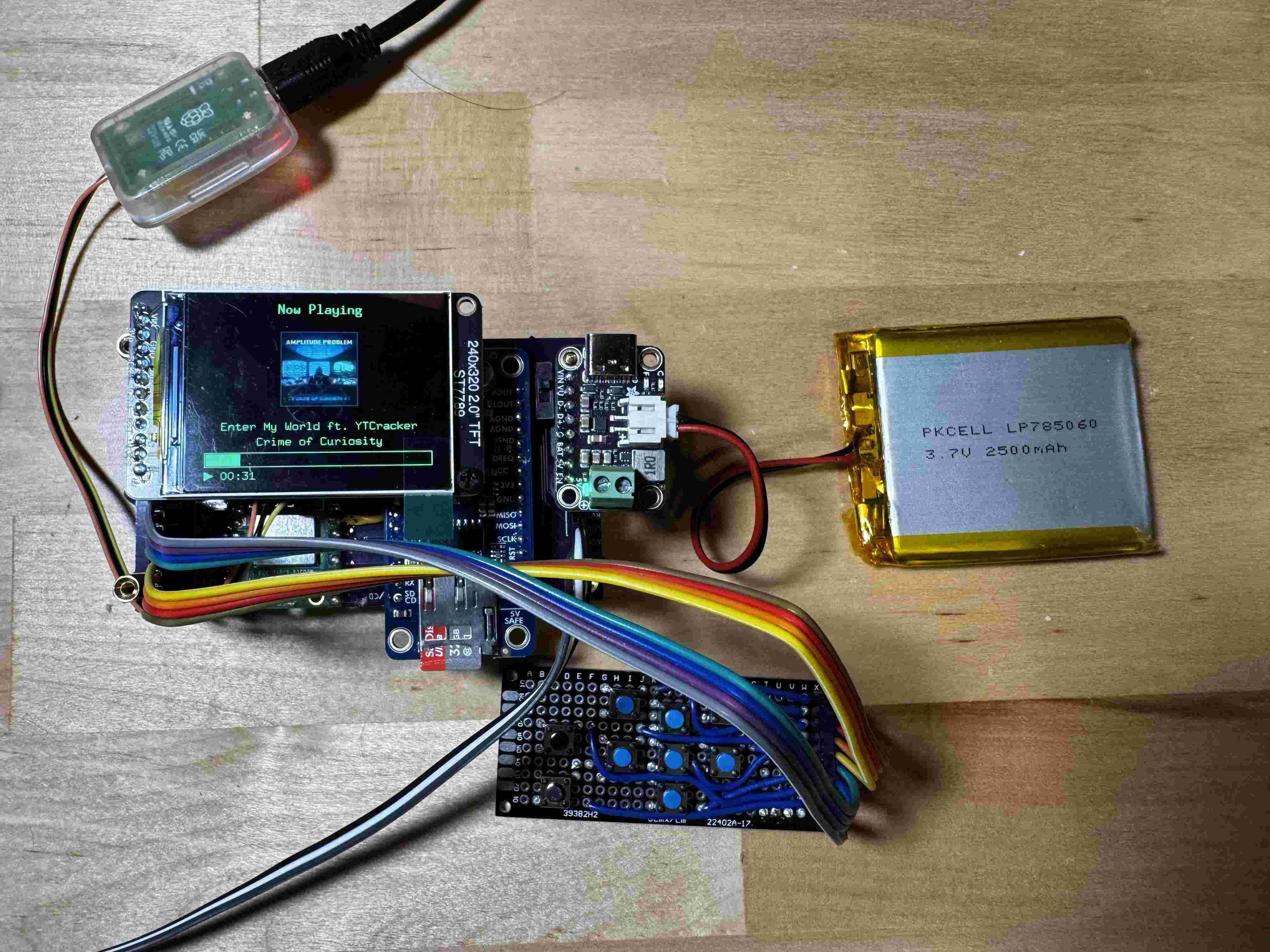
I built a small test board with simple buttons & updated the firmware to enable pull-ups. With some software support, they work within the menu system:
Next Steps
I’m now working on an initial version of the board, with spots for all the existing components! Stay tuned.